|
The ISP Column
A column on things Internet |
||
|
Other Formats:
|
||
Chipping Away
August 2023
Geoff Huston
This is part of a personal commentary on the meetings at the July 2023 meeting of the Internet Engineering Task Force (IETF 117). If you want to know what was presented and the comments at the mic see the IETF 117 meeting archive.
The ACM/IRTF Applied Network Research Workshop is always an interesting segment in the IETF week, and the workshop held during IETF 117 was no exception. The keynote presentation, entitled "It’s the End of DRAM As We Know It" by Philip Levis of Stanford University has put forward some interesting perspectives on the state of the advanced edge of the silicon chip design and fabrication process, which I would like to reflect upon here.
The computer industry has been an iconic outcome of the twentieth century, starting the century with work on the foundations of mathematics (“Principia Mathematica” by Alfred Whitehead and Bertrand Russell) which led to work logic systems and formal languages, then Kurt Gödel’s incompleteness theorem on the limits of formal systems. This led to further exploration of formal systems and the issues of computability with notable contributions from Alan Turing and Alonzo Church in the 1930's. The work on code breaking in the 1940’s with major contributions by Alan Turing lead to programmable computers. These computing devices quickly found a home in the defence industry for various military applications and followed by adoption by the world or commerce and ultimately into the consumer market. There have been many actors in this story over the past century, both an individuals and institutions, but within the story of computers Bell Laboratories, the research arm of the American phone company AT&T, has a towering presence.
Vacuum tube computers were used in the development of computers to perform cryptanalysis of wartime cipher codes in the 1940's and upon the conclusion of the war the efforts continued with defence support to design and build larger and more capable devices. But these vacuum tubes were bulky, power hungry, unreliable, and slow. Bell Labs started working on a faster alternative, starting with diodes using germanium semiconducting crystals. A Bell Labs research team lead by Willian Shockley took on the task of taking the germanium diode and seeing how it could be used to construct a triode. Bell Labs announced the point-contact transistor in 1947 and the bipolar junction transistor in 1948. These transistors were faster and far more reliable than vacuum tubes, and demand was so high that within two years the transistor was being fabricated in volume. Through the 1950's transistors were used to replace vacuum tubes in telephone switches, consumer radios and computers. For example, the IBM 7070 was produced in 1958 as a transistor-based device. In this generation of semiconductors, the transistor simply replaced the vacuum tube in electric circuits, allowing for a smaller and more reliable device that required less power to operate. Transistors were quickly used in small portable radios by Sony, and into the munitions guidance system used by missiles in the US military, and all things in between!
In the late 1950's Bell Labs announced the invention of the Field Effect Transistor based on a metal-oxide-semiconductor (MOSFET). It was the first truly compact transistor that could be miniaturised and mass-produced cost efficiently. MOSFET led to the idea of integrating a number of transistors into the same block of semiconductor material, effectively producing a multi-transistor circuit in a single semiconductor package.
The invention of the transistor and its refinement into monolithic integrated circuits was one the towering achievements of the twentieth century. It stands alongside the development of the material and manufacturing technologies of the late 18th century that led to the integration of machinery into the production cycle and leading to the industrial revolution that had a profound revolutionary impact on western European society at first and ultimately on the entire human population. It has been argued that the onset of the industrial revolution is the most important event in human history since the domestication of animals. Over its 75-year history the transistor has heralded a similar social revolution that is rebuilding the world in a post-industrial framework.
So far, the silicon technology at the heart of this revolution has been truly prodigious. The processes of assembling silicon wafers and the superimposition of tracks and gates into increasingly complex circuits has proved to be susceptible to continual refinement. In 1965, just 6 years after the invention of the MOSFET transistor and integrated circuits, Fairchild's Gordon Moore observed that the number of discrete components that could be placed into an integrated circuit was doubling every year, and he predicted that this would continue for another decade. This implied that over ensuring ten years it would be possible to place one thousand times the number of transistors into an integrated circuit than was possible in 1965. But there was more to it than just the device count. The experience with vacuum tube valves was hardly encouraging. If you used valves with a mean in-service lifetime of 1,000 hours, and your device had 10,000 valves then you could expect a valve failure every 6 minutes on average! The more valves you used, the more you compromised the operational lifetime of the device.
With silicon the story was entirely different. Not only could they be manufactured in smaller and small sizes, but the declining size also implied a lower power consumption, an improved switching speed and a longer anticipated lifetime. There was no vacuum seal to maintain, no heat to manage and no large amperage to shunt through the device the heat every valve. The silicon industry was in factor delivering smaller, faster, cheaper, and more reliable, all at once! When he was asked about his prediction a decade later, in 1975, Gordon Moore produced slightly modified forecast of a doubling of the device count every two years. And once again his prediction matched the ensuing developments in chip fabrication. And this has continued, in that this exponential increase in the device count on silicon wafers has been sustained for the ensuing fifty years. From tens of transistors in the early 60s, we are now looking at individual silicon chips with some 100 billion transistors in the mid-2020s, and we are peering into a near future of trillions of devices on a single chip.
Technically, that’s a truly remarkable achievement, and I'd like to look at the larger question of sustainability of Gordon Moore’s forecasts in the years to come, but it’s worth pausing for a second to catch our breath and look at the current economics and politics of silicon chip fabrication.
Silicon Business and Politics
Gartner claim that worldwide semiconductor revenue was some $602 billion in 2022. The 10 largest chip vendors accounted for 46% of this revenue. The largest market share, or 10.9% of 2022 semiconductor revenue, is held by the Korean firm Samsung Electronics, followed by the US firm Intel with 9.7% market share and then the Korean form SK Hynix with 6.0% market share by revenue. However, who is selling chip, who is designing these chips, and who is actually making (or “fabricating”) these chips are all different stories. Overall, one third of 2022 sales revenues are attributed to American chip providers, yet no significant volumes of leading semiconductors are fabricated in America. A similar view can be seen when looking at the microprocessor production volumes (Figure 1).
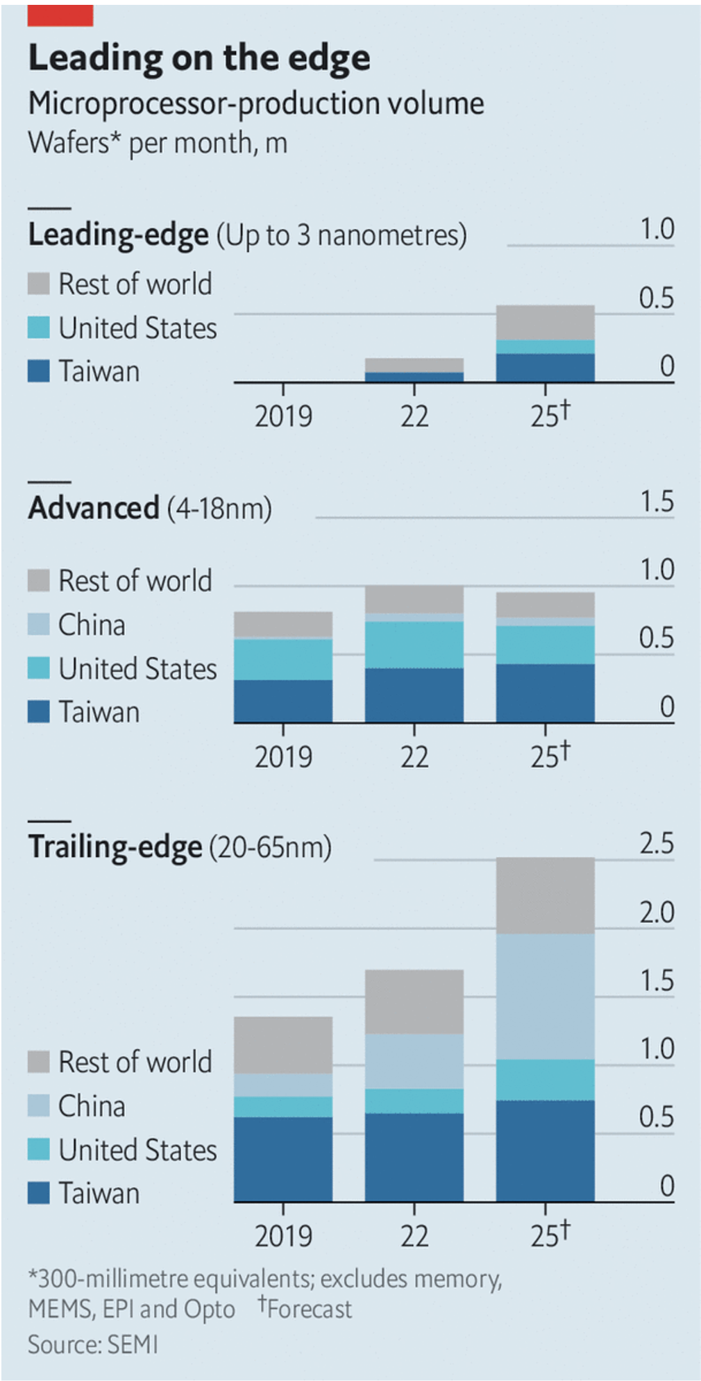
Figure 1 – Microprocessor Production Volumes – From The Economist
A significant proportion of the fabrication of silicon chips occurs in Taiwan, and at plants operated by the Taiwan Semiconductor Manufacturing Company (TMSC). Taiwan made an offer to former Texas Instruments engineer Morris Chang some 40 years ago to lure him back to Taiwan to establish the most advanced semiconductor manufacturing operation in the world. The key feature of this operation was that it had no intention of designing its own chips, but would operate as a foundry, making chips to the specifications of others. TSMC is large. It is the most valuable company in Asia at the moment, accounting for some 5% of the Taiwanese GDP and 7% of its electricity consumption. It operates 4 “giga-factories” in Taiwan as well as a number of “mega-factories.” The company fabricates some 60% of the semiconductors used today, and 90% of the most advanced semiconductors. This is a critically important company in today’s digital world, and the unresolved political tensions between Taiwan and China are a cause for some perceptions of heightened risk. In 2022 Warren Buffer purchased more than $4B of TSMC shares, and in 2023 he sold them, at a loss, citing concerns over TSMC’s location. The risk of a near term confrontation between Taiwan and China is too great, according to Warren Buffet.
Obviously, this is a highly valuable business. But its more than just the value of the products that this industry produces that’s important. The robustness of the supply chains is also critical. There have been some interruptions to chip supplies in recent years, such as the Covid period which saw the combination of reduced production due to workforce interruptions, and a period of drought in Taiwan which reduced the supply of water for chip fabrication. When there is a hiatus to chip production many other industries feel the impact, as there were no feasible substitutions for silicon chips. For example, some car manufacturers were forced to halt their production lines due to the3 lack of chips, which cause a ripple in the supply chains for the auto industry and so on. Some years later we are still seeing instances where the supply systems are disrupted and the wait period for certain goods are still disrupted. There is also the ever-present issue of political tensions, trade sanctions, and even the possibility of exclusion into military actions that could harm the existing supply channels.
This concern about the vulnerability of silicon chip supply lines to disruption in a globalised industry is by no means a recent concern. In the 1980's tension emerged over the emerging Japanese semiconductor industry, which was able to make DRAM chips with higher reliability and lower cost than their US competitors. Various measures were enacted to try and protect the declining US silicon fabrication industry from what was perceived as unfair Japanese competition. The manufacture of DRAM is a classic commodity business where production efficiencies and continual re-investment in new fabrication facilities is a key factor. The Japanese DRAM production peaked in the late 1980s and has waned since, replaced by advanced fabrication facilities located in Taiwan, Korea and Singapore. One of the side effects of Moore’s Law is that to keep ahead of the competition the existing providers need to continually reinvest in new production infrastructure and any misstep in either the choice of new technologies, or the timing of its introduction will be harshly punished by the market.
These days every aspect of modern society is dependent on the silicon industry. As a recognition of the critical level of dependence of the US economy on the semiconductor supply chains, and a desire to reduce the level of vulnerability to externalities that can interrupt these supply chains, in 2022 the US enacted a federal funding package of a total of $50B to lure chip fabrication back to the US, using a similar form of financial inducement that had lured the semiconductor manufacturing activity away from the US and ultimately into Taiwan, Korea and Singapore. This US funding program has resulted in announcements of some $200B investment in the construction of US chip fabrication plants, with the largest producer of leading chips, TMSC, announcing the construction of two new plants in Arizona, one to produce 5nm chips and the second to produce 3nm chips. Samsung has announced a $17B investment in Texas, and Intel is set of spend $40B on four plants in Arizona and Ohio. The overall objective from these investments is to manufacture a little under one fifth of the world's leading chips in the US once these plants are constructed and swing into production in 2025 (Figure 2).
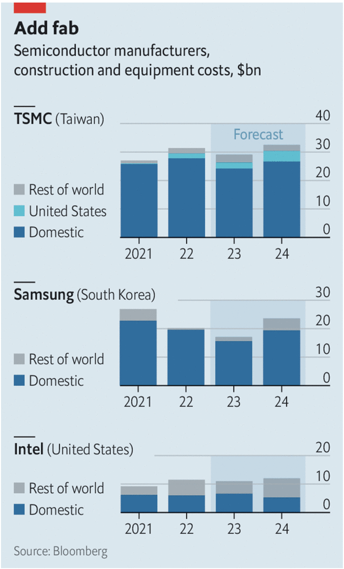
Figure 2 – Semiconductor construction and equipment costs – From The Economist
Industrial production facilities used to be located adjacent to its primary inputs, be it iron ore, coal, hydro energy, or a skilled labour force, but in the silicon fabrication business this is not necessarily the case. Silicon and the trace levels of rare earth materials can be readily shipped to most locations, so the relative cost elements in operating a chip fabrication plant are down to the cost of the plant constructions the cost of labour and the availability of large amounts of water. The US locations are not exactly optimal in any of these three factors, particularly in Arizona where a number of these plants are being constructed. It's taking some 900 days to construct a plant in the US dues to a greater level of regulatory clearances that are required, compared to around 650 days in Taiwan and Korea, access to large amounts of clean water is an ongoing issue for Arizona, and they'll need to use large scale water recycling and filtration plant to provide the large volumes of ultra-clean water required by the manufacturing process. And US labour costs were one of the motivations for moving chip fabrication to Asia in the first place. All of these issues are by no means intractable, and can all be addressed with sufficient capital, but it does mean that the desire for greater levels of domestic chip fabrication comes at a cost. This is not an issue for the US alone. The European Union recently approved the European Chips Act, a €43 B subsidy plan to double its chipmaking capacity by 2030, with a goal of at least 20% of world production of semiconductors in Europe by 2030, and support via a European Alliance on semiconductor manufacture. Germany has also committed to paying a third of the cost for a fab plant to be built by Intel in Magdeburg. TMSC has committed €3.5 B towards setting up a chip factory in Dresden, Germany. This is the first plant in Europe for TSMC, and its third outside Taiwan and China.
However, while the existing plant operators are willing to respond to such public sector initiatives to boost domestic chip fabrication capability in America and Europe, the bulk of the capital investment in new plants will continue to be in Taiwan for TMSC and Korea for Samsung. Consequently, the majority of the leading chips will continue to be made in Asia, principally in Taiwan and Korea. There is still a major demand for chips with a lower gate density. Today one fifth of these non-leading (more than 28nm and not using EUV lithography) chips are fabricated in China, and in the coming couple of years this proportion is likely to increase to one third of all such chips.
With all this effort to diversify the fabrication of silicon chips there is now the contradictory outcome that a single supplier lies at the heart of this industry. ASML, a Dutch multinational corporation, specializes in the development and manufacturing of photolithography machines, using component technologies drawn from the Americas and Europe. As of 2022 it is the largest supplier for the semiconductor industry and the sole supplier in the world of extreme ultraviolet lithography (EUV) photolithography machines that are required to manufacture the most advanced chips. These machines produce light in the 13.5 nm wavelength range when a high-energy laser is focused on microscopic droplets of molten tin to produce a plasma, which then emits EUV light. The light is bounced off mirrors in a vacuum onto the surface of a silicon wafer to deliver the designs for the chip. ASML's best-selling EUV lithography system costs up to $200 million. As of 2022, ASML has shipped around of these 140 systems. They are working on the next generation of EUV systems, with the first shipments expected to take place at the end of 2023.
The increasing specialisation of machinery required to keep pace with Moore’s law has meant that the industry operates with high research and development costs as well as costs in the manufacture of extremely high precision equipment. The result is that many companies have dropped out of the market, both in making fabrication systems themselves and in the manufacture of various components of these systems, and AMSL now finds itself in the position of being the only company manufacturing EUV lithography systems. If the underlying political issue was one of points of critical vulnerability in the silicon supply chain, then it’s unclear to me that this has really been addressed.
But Moore’s law has taught us something else as well, namely that leadership in the technology of chip manufacture is transitory, and each generation of the fabrication process lasts for 5 – 10 years at most. This means that there is a brief window of market leadership that allows a chip vendor to charge a premium price for the most advanced chips before it is superseded by the next generation, and in this brief period it must not only weather the transitory cycles of glut and scarcity in chip supply, but also recoup the years of lead-up research costs that had enabled this particular technology in the first place. What this means is that this industry is incapable of sustaining many advanced independent chip fabricators. The old model of a single enterprise designing and fabricating its own chip set is over, and the business model of specialised fabricator operating on a “bring-your-own-design” model is now dominant in the industry. It’s unlikely that this situation will change in the foreseeable future.
Even when we split the role of chip design from fabrication it’s still a challenging business to sustain in a profitable manner. Up front research and development costs are high, yet the market appetite for million-dollar chips is extremely limited. The “core” of the leading market is for micro-processors that retail for between $5,000 for $10,000 per chip, which means that the upfront R&D costs need to be recouped over large volume runs. But if the current set of chips is under constant threat by advances in Moore’s Law, then each incarnation of a “leading” chip is under threat from the next set of chips, and the time over which such a chip can command premium prices can be measured in months and not years (see Figure 3). The inevitable result of a commodity-based industry where the economies of scale are dominant is the amalgamation of the industry until all that's left is a single industry. This characterises the state of the leading edge silicon fabrication process, where AMSL and TMSC both find themselves as the sole player in their chosen area of activity, namely AMSL in EUV lithography and TMSC in fabrication.
Maybe the silicon industry would calm down a little and embrace slightly more economic stability if we backed off from the inexorable cycle of disruptive changes being caused by the continual process of refinement in scale, power, speed and cost of these chips. Moore’s Law is a harsh business master. However, here it may be a case of being very careful of what we may wish for!
Can Moore’s Law Continue?
If we look at the successions of refinement to the MOSFET silicon chip it is once more time to ask the question of whether we have reached the end of Moore’s law. The plot of the advanced chip feature size over time is shown in Figure 3.
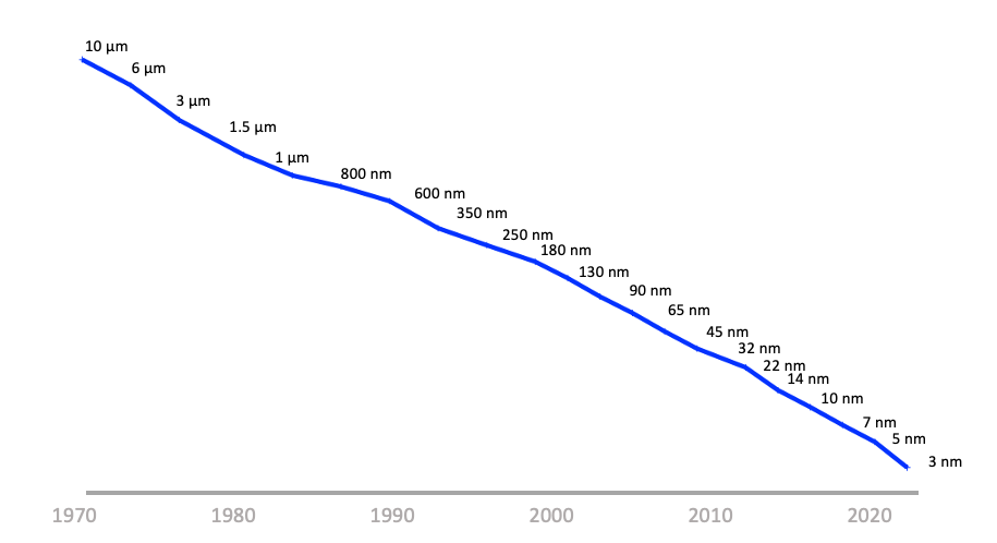
Figure 3 – Silicon Feature size over time (From Wikipedia: 3_nm_process)
A similar time series plot shows the number of transistors in microprocessors over time (Figure 4). This plot ends in 2019 and since that time there have been a number of major advances including Apple’s M2 Ultra processor chip that uses 134 billion transistors, and Micron’s V-NAND memory chip that uses 5.3 trillion transistors in a stacked package of sixteen 232-layer 3D dies.,/P.
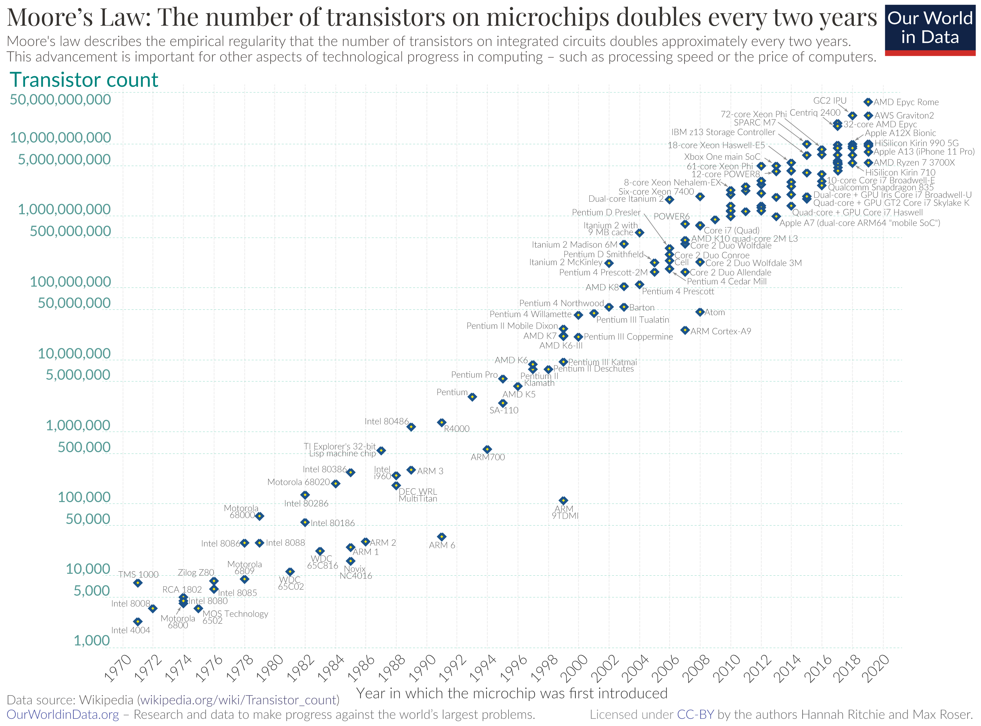
Figure 4 – Transistor count in microprocessors up to 2019 - By Max Roser, Hannah Ritchie, CC BY 4.0
Historically, these numbers represented the width of conducting tracks etched into the silicon substrate, but this is no longer the case for the extremely advanced ships. Chip manufacturers tend to use these size numbers to represent a combination of factors, including power consumption, switching speed and transistor density. For example. TMSC has stated that its 3nm chips will operate with a reduced power consumption of 25%-30% at the same speed, or a switching speed increase of 10%-15% at the same power, and an increase of transistor density of 33%. Samsung has made similar claims about its 3nm process, with a drop in power consumption by 45%, a lift in performance by 23% and an improvement in density by 16% as compared to the 5nm process.
The recent achievement of higher date densities has been achieved not by simply decreasing the track widths on the silicon substrate, but by creating three-dimensional gate structures rather than planar gates (the so-called “finFET” gate). This gate design has been the dominant form of gate in the 22nm and smaller chip designs. This results in the ability to create higher density of features in a silicon wafer, but with a cost of an increased number of process steps to construct the chip, and this has an inevitable cost implication. One way to express this is in the trend of cost per gate (Figure 5)
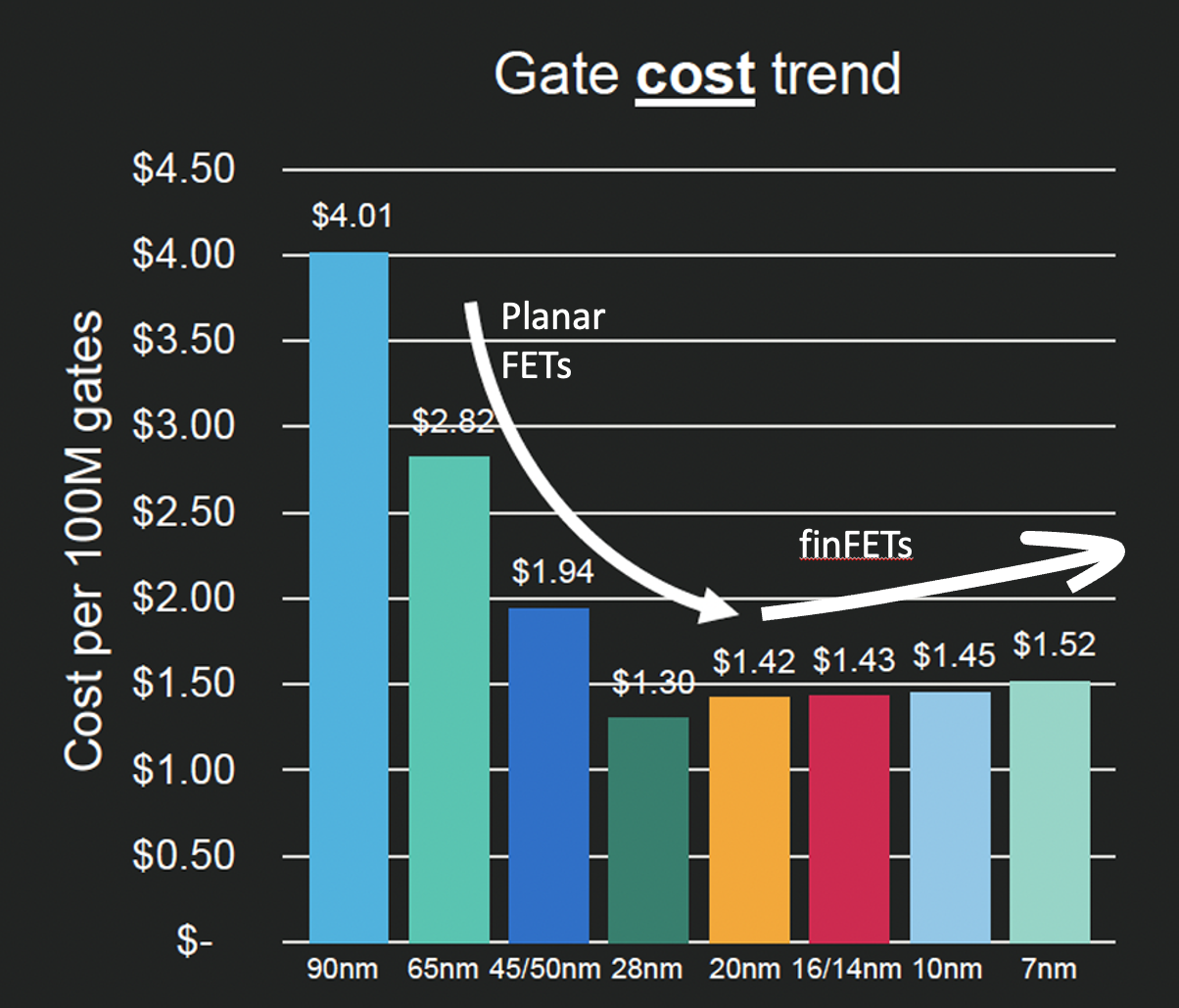
Figure 5 – Gate cost trend (From Marvell Investor Day 2020 presentation)
Whereas in planar FETs the decreasing size of features was achieved with a corresponding decrease in the unit cost, the finFET model uses more processing steps, and the unit cost of gates is increasing as the feature size decreases. Since the 28nm chip size in 2010 smaller is no longer cheaper in terms of cost per silicon gate.
This is reflected in the cost and performance of silicon hardware. For example, the comparison of memory chips over the past 25 years in shown in Table 1. While the memory systems have greater capacity and throughput, the access latency has flattened out and most critically the cost per unit of memory has gone past a minimum and started to increase with DDR5 memory (Table 1).
| Version | Year | Throughput | Latency | $/Gbyte |
| DDR | 1998 | 3.2GBps | 134ns | $78 |
| DDR2 | 2003 | 8.5GBps | 122ns | $9 |
| DDR3 | 2007 | 17GBps | 79ns | $3 |
| DDR4 | 2014 | 26GBps | 74ns | $2 |
| DDR5 | 2020 | 57GBps | 72ns | $3 |
Table 1 – DRAM performance and unit price over time
What about processor chips? DRAM is in many ways a simple design, as each memory cell is a gate and a capacitor. In the case of processors, the design of the chip is important, and squeezing better performance from a chip is a combination of smaller gates allowing more processor cores to be placed on a single chip coupled with the integration of processing logic and caches. Table 2 shows the evolution of the AMD processor chip set over the past five years.
| Year | Processor | Cores | Transistors | Clock | Cost | $/core |
| 2019 | Rome | 64 | 40B | 2.25GHz | $6,950 | $109 |
| 2022 | Milan | 64 | 26B | 2.20GHz | $8,800 | $138 |
| 2022 | Genoa | 96 | 90B | 2.40GHz | $10,625 | $110 |
| 2023 | Bergamo | 128 | 82B | 2.25GHz | $11,900 | $92 |
Table 2 – CPU performance and unit price over time – AMD processors
Note that the clock frequency is largely stable over this period. This has been the case since 2005. Prior to this so-called “Dennard scaling” applied to MOSFET devices, where the leverage of smaller gate size coupled with lower power and lower capacitance lead to an increase in clock frequency, as predicted in a 1974 paper co-authored by Robert Dennard. The issue is that at smaller gate size there is an increase in current leakage which generates heat, and the resulting thermal runaway increases the energy costs. The resultant picture of processor clock speeds is shown in Figure 6.
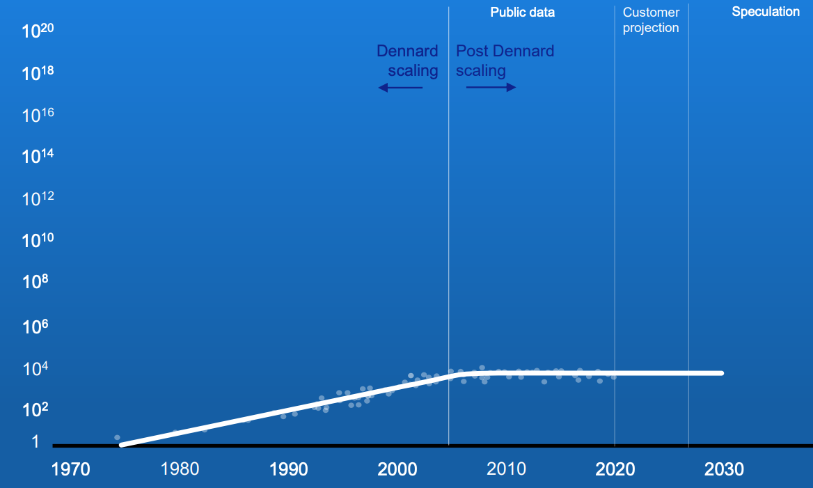
Figure 6 – Processor Clock Frequency over time – ASML Investor Briefing September 2021
Given that the processor clock speed has remained steady for the past twenty years the way that performance has been improved in this period is to increase the number of cores within the chip so that the chip can perform various multi-tasking roles more efficiently.
It’s not clear that we have optimised this model of finFETs as far as we could possibly go. There is likely to be further potential in the use of 3D silicon structures, and finFETs are the start of another generation of special density improvements in chip design, termed “Gate-All-Around” (Figure 7).
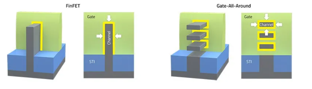
Figure 7 – Gate-All-Around design (from SemiEngineering)
By shifting to layered designs and going vertical in gate design it is possible to reap further increases in gate density in terms of the density of gates per square mm on the silicon substrate, which can offer some prospect for further improvements in chip performance coming years. But even this model runs into performance limitations at 2nm, and alternatives are being researched. While novel structures such as carbon nanotube FETs and vertical transport FETs can deliver amazing electrical properties, they are extremely difficult to fabricate. As a result, most of these approaches will never move from lab to fab. Realistically, the industry can only afford to back one fabrication candidate.
However, the largest area of potential improvement in processor chips lies in the area of system design within the chip. The way in which the various cores are placed in the ship, the management of heat, the integration of nearby cache memory with processing capability on the chip offer the potential for further power reduction and the potential for system performance improvements (Figure 8).
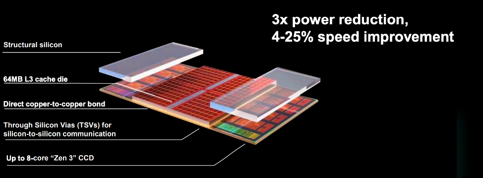
Figure 8 – AMD 3D chiplet design – ASML Investor Briefing September 2021>/a>
But once again this comes at a price, and its's not just the increased number and complexity of production steps in fabrication that presents us with cost escalation. The average cost of designing a 28nm chip has been reported to be some $40 million. By comparison, the cost of designing a 7nm chip is around $200 million, a 5nm processor device is some $400 million and a 3nm design will cost up to $600 million.
However, this upfront cost is defrayed against high volume production runs, and while the costs look forbidding, its useful to refer to the price information in Table 2 and note that despite the escalating total cost of the design and production of the processor chip, the unit cost of each core is still falling. The $12,000 cost of the most advanced AMD chip in 2023 is the equivalent to a price $2,000 in 1975 dollars, or 40 times the cost of a Zilogics Z80, but with a processor clock that runs at 1,000 times faster, and with 128 cores, or, in rough terms, an improvement in the unit cost of processing of 3,200 times!
While the investments are high to keep on improving chip performance, there is still some cause for optimism that all is not yet over with Moore’s Law, and we can continue to extract further improvements in chip performance by looking at the overall system design, rather than fixating on just the size of individual gates or on the clock speed. AMSL’s position in 2021 was certainly upbeat in terms of their predictions over the coming few years (Figure 9).
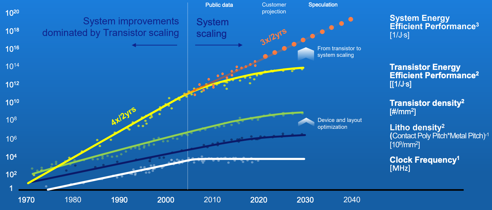
Figure 9 - AMSL report on silicon performance – ASML Investor Briefing September 2021
However, some physical issues are coming into play in this admittedly rosy view of the future. Silicon atoms are 0.2nm in diameter, and if we are looking at silicon structures of a 1nm dimension that implies that we are looking at structure of 4 - 5 atoms in size. When you add the issue of electron tunnelling due to quantum effects then constructing high speed deterministic switching systems at this size becomes an extremely challenging objective. And so far, we have not even touched upon the production issues of maintaining a high yield level of chips when the layer stack count increases, the number of discrete production steps extends into the thousands, and the number of gates per chip heads into the tens of trillions.
However, it would be foolhardy to assert this is an impossible task. The very idea of a silicon chip with 90B gates operating with a 3 GHz clock would’ve been readily dismissed as totally impossible when we commenced this journey with the transistor back in 1949!
Implications for Networks
The communications industry has benefitted greatly from the advances in silicon, both in terms of on-chip processing capacity and in fast memory. The digital signal processing task of encoding a bit stream to modulate an optical signal, and the reverse process of taking an analogue optical signal and decoding into the original bit stream is tightly coupled to the complexity and speed of the processing that can be performed on the chip, which, as shown in Table 3, has been related to available processing capability in silicon.
| Year | Mode | Baud | Capacity/Lambda | Cable Capacity | DSP |
| 2010 | PM-QPSK | 32 GBd | 100G | 8T, C-Band | 40nm |
| 2015 | PM-16QAM | 32 GBd | 200G | 19.2T, Ext C | 28nm |
| 2017 | PM-32QAM | 56 GBd | 400G | 19.2T, Ext C | 28nm |
| 2019 | PM-64QAM | 68 GBd | 600G | 38T, Ext C | 16nm |
| 2020 | PS-PM-64QAM | 100 GBd | 800G | 42T, Ext C | 7nm |
| 2022 | PCS-144QAM | 190 GBd | 2.2T | 105T, Ext C | 5nm |
Table 3 – Coherent Fibre Evolution
If 288QAM is ever going to be viable then it appears that a significantly greater processing capability is required over what can be obtained from 5nm silicon. This implies that fibre capacity beyond 2.2Tbps per wavelength may well be dependent on 2nm silicon for the DSP function.
As well as processor limits there is the issue of memory speeds not getting any faster. The way we’ve tried to design around this limitation is to increase the level of parallelism. The latest such offering is High Bandwidth Memory (HBM) with 16 x 64-bit channels, which requires 1,024 data lines. This level of parallelism is beyond the capability of printed circuit boards, so it’s logical to package the HBM memory module and the processor on a single substrate, binding memory and processing on a single chip. This, in turn, leads to a direction of increasing levels of customisation of silicon chips, balancing the number of CPU cores on the chip against the amount of space devoted to on-board HBM. Rather than using conventional general purpose processing chips with DDR memory on the PCB, we will be looking at various combination of processing and memory capabilities to create a more precise match the demands of the application with the design of the silicon.
Conclusion
We’ve been living long enough with the prodigious outcomes of Moore’s Law in terms of the continually decreasing cost and simply overwhelming abundance of storage and processing capability that it’s now going to take some effort to recalibrate both our thinking and our business models as the pace of this form of technology leverage slows down.
We haven't reached the end of Moore’s Law by any means, but as we move away from the process of continual refinements in the size, power requirements and switching speed of transistors, while still using a basic planar FET design we are entering into a more complex space. The use of finFETs and all-around-gates introduce a view of the silicon chip as a 3D lattice. There are some benefits in further improvements in size, power and speed in going down this path, but the cost lies in the significantly increased complexity of the fabrication process and the pressure on overall chip yields.
While its challenging to innovate on the design of DRAMs, it is still possible to innovate in the design of processors. By folding in wide bus memory and interface capabilities into the processor it is possible to design chips with an improved processing capability for particular classes of applications. We may be nearing the end of the high-speed general purpose utility silicon processor, replacing it with system designs that are specifically designed to perform well when undertaking a particular class of processing tasks.
The computing environment may see some radical changes over the next decade or so as a result, and this may also have a major impact on the design of networks and the relationship between the network’s communication elements and its processing and storage elements.
![]()
Disclaimer
The above views do not necessarily represent the views of the Asia Pacific Network Information Centre.
![]()
About the Author
GEOFF HUSTON AM, B.Sc., M.Sc., is the Chief Scientist at APNIC, the Regional Internet Registry serving the Asia Pacific region.